|
|
555 Timer - Frequency and Duty Cycle Calculator
Enter values for R1, R2, and C and press the calculate button to solve for positive time interval (T1) and negative time interval (T2). For example, a 10K resistor (R1) and 100K (R2) and 0.1 uF capacitor will
produce output time intervals of 7.62 mS positive (T1) and 6.93 mS negative (T2). The frequency will be about 70 Hz. R1 should be greater than 1K and C should be greater than .0005 uF. Scroll down page for basic
555 information (pinout and two basic circuits).
Positive Time Interval (T1) = 0.693 * (R1+R2) * C
Negative Time Interval (T2) = 0.693 * R2 * C
Frequency = 1.44 / ( (R1+R2+R2) * C)
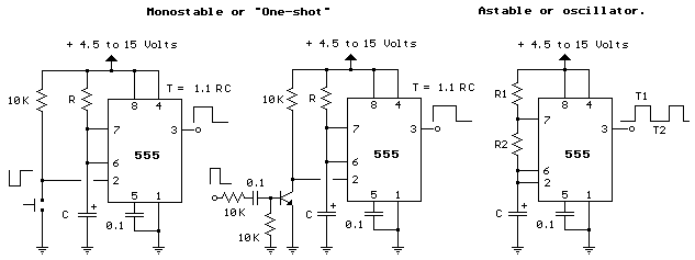
The 555 Timer
First introduced by the Signetics Corporation as the SE555/NE555 about 1971.

Pin connections and functions: (See schematic below for basic circuits)

Pin 1 (Ground)    - The ground (or common) pin is the most-negative supply potential
                    of the device, which is normally connected to circuit common when
                    operated from positive supply voltages.

Pin 2 (Trigger)   - This pin is the input which causes the output to go high and begin
                    the timing cycle. Triggering occurs when the trigger input moves
                    from a voltage above 2/3 of the supply voltage to a voltage below
                    1/3 of the supply. For example using a 12 volt supply, the trigger
                    input voltage must start from above 8 volts and move down to a
                    voltage below 4 volts to begin the timing cycle. The action is
                    level sensitive and the trigger voltage may move very slowly. To
                    avoid re-triggering, the trigger voltage must return to a voltage
                    above 1/3 of the supply before the end of the timing cycle in the
                    monostable mode. Trigger input current is about 0.5 microamps.

Pin 3 (Output)    - The output pin of the 555 moves to a high level of 1.7 volts less
                    than the supply voltage when the timing cycle begins. The output
                    returns to a low level near 0 at the end of the cycle. Maximum
                    current from the output at either low or high levels is
                    approximately 200 mA.

Pin 4 (Reset):    - A low logic level on this pin resets the timer and returns the
                    ouput to a low state. It is normally connected to the + supply
                    line if not used.

Pin 5 (Control)   - This pin allows changing the triggering and threshold voltages by
                    applying an external voltage. When the timer is operating in the
                    astable or oscillating mode, this input could be used to alter or
                    frequency modulate the output. If not in use, it is recommended
                    installing a small capacitor from pin 5 to ground to avoid
                    possible false or erratic triggering from noise effects.

Pin 6 (Threshold) - Pin 6 is used to reset the latch and cause the output to go low.
                    Reset occurs when the voltage on this pin moves from a voltage
                    below 1/3 of the supply to a voltage above 2/3 of the supply.
                    The action is level sensitive and can move slowly similar to the
                    trigger voltage.

Pin 7 (Discharge) - This pin is an open collector output which is in phase with the
                    main output on pin 3 and has similar current sinking capability.

Pin 8 (V +)       - This is the positive supply voltage terminal of the 555 timer IC.
                    Supply-voltage operating range  is +4.5 volts (minimum) to +16
                    volts (maximum).


The pin connections for the 556 which is a dual 555 timer (2 in one package) are
shown in table below. For example, the two outputs for the two timers of the 556 are
on pins 5 and 9 which correspond to the output pin 3 of the 555.

                            555      556 timer #1        timer #2
            -------------------------------------------------------
              Ground         1                  7               7
              Trigger        2                  6               8
              Output         3                  5               9
              Reset          4                  4               10
              Control        5                  3               11
              Threshold      6                  2               12
              Discharge      7                  1               13
              + Power Vcc    8                  14              14
            -------------------------------------------------------

The schematics below show the two basic circuits for the 555 timer.
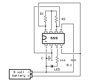
Below is a pictorial view of the 555 timer wired as a LED flasher and powered with a 9 volt battery. The LED will turn on during time T1 and off during time T2.
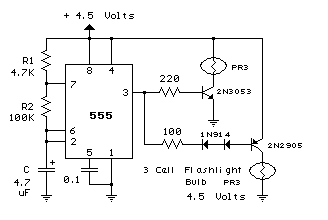
The 555 circuit below is a flashing bicycle light powered with three C or D cells (4.5 volts). The two flashlight lamps will alternately flash at a approximate 1.5 second cycle rate. Using a 4.7K resistor for R1
and a 100K resistor for R2 and a 4.7uF capacitor, the time intervals for the two lamps are 341 milliseconds (T1, upper lamp) and 326 milliseconds (T2 lower lamp). The lamps are driven by transistors to provide
additional current beyond the 200 mA limit of the 555 timer. A 2N2905 PNP and a 2N3053 NPN could be used for lamps requiring 500 mA or less. For additional current, a TIP29 NPN and TIP30 PNP could be used up to 1
amp. A PR3 is a 4.5 volt, 500 mA flashlight bulb. Two diodes are placed in series with the PNP transistor base so that the lower lamp turns off when the 555 output goes high during the T1 time interval. The high
output level of the 555 timer is 1.7 volts less than the supply voltage. Adding the two diodes increases the forward voltage required for the PNP transistor to about 2.1 volts so that the 1.7 volt difference from
supply to the output is not enough to turn on the transistor. You can also use an LED in place of the two diodes as shown in the lower schematic.
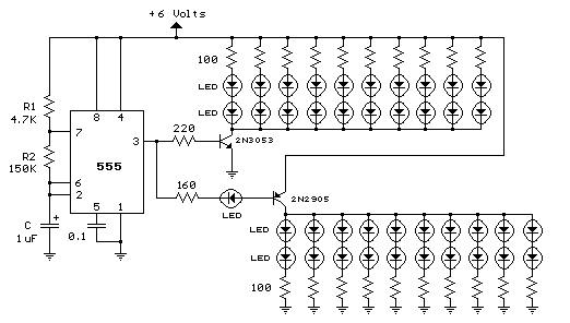
40 LED Bicycle Light
The 555 circuit below is a flashing bicycle light powered with four C,D or AA cells (6 volts). Two sets of 20 LEDs will alternately flash at approximately 4.7 cycles per second using RC values shown (4.7K
for R1, 150K for R2 and a 1uF capacitor). Time intervals for the two lamps are about 107 milliseconds (T1, upper LEDs) and 104 milliseconds (T2 lower LEDs). Two transistors are used to provide additional current
beyond the 200 mA limit of the 555 timer. A single LED is placed in series with the base of the PNP transistor so that the lower 20 LEDs turn off when the 555 output goes high during the T1 time interval. The high
output level of the 555 timer is 1.7 volts less than the supply voltage. Adding the LED increases the forward voltage required for the PNP transistor to about 2.7 volts so that the 1.7 volt difference from supply
to the output is insufficient to turn on the transistor. Each LED is supplied with about 20 mA of current for a total of 220 mA. The circuit should work with additional LEDs up to about 40 for each group, or 81
total. The circuit will also work with fewer LEDs so it could be assembled and tested with just 5 LEDs (two groups of two plus one) before adding the others.
|
|