Semiconductors:
Diodes & Transistors
In the early days of electricity there were only two groups of material: insulators and conductors. Insulators are matters, which do not allow the flow of electric current through them. Glass, porcelain, dry air and dry wood are well known insulators. Metals are known to be good conductors, with copper and silver among the best. The conductivity of a particular material depends on the number of free electrons present in it.
There is another group of material known as semiconductors. Semiconductors like germanium and silicon are bad conductors of electricity in their purest form. But when certain impurities (indium or arsenic, which have a slightly different atomic structure from that of germanium or silicon) are added in the form of carefully controlled quantities, either an increase of free electrons or deficiency of electrons results. A semiconductor is called an n-type semiconductor where conduction takes place by reason of excess free electrons. A semiconductor is called a p-type semiconductor where conduction takes place due to freely moving ‘holes’ (positively charged) which replace electrons displaced by random electron movement in the material.
DIODES
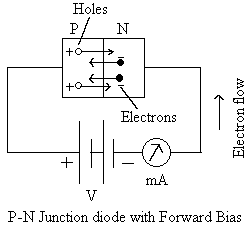
When pieces of p-type and n-type semiconductors are joined together, a p-n junction results. Flow of electric current through such a junction is possible only when the positive pole of the battery (voltage source) is connected to the p-type semiconductor and the negative pole to the n-type semiconductor.
This is called the “forward biased” condition. In this condition, positively charged holes are repelled by the battery voltage towards the junction between p and n type material. Simultaneously, the electrons in the n-type material are repelled by the negative battery voltage toward the p-n junction. Despite the presence of a potential barrier at the p-n junction, which prevents electrons and holes from moving across and combining, under the influence of the electric field of the battery the holes move to the right across the junction
and the electrons move to the left. As a result, electrons and holes combine and for each combination of that takes place near the junction, a covalent bond near the positive battery terminal breaks down, an electron is liberated and enters the positive terminal. This action creates a new hole which moves to the right toward the p-n junction.
At the opposite end, in the N-region near the negative terminal, more electrons arrive from the negative battery terminal and enter the n-region to replace the electrons lost by combination with holes near the junction. These electrons move toward the junction at the left, where they again combine with new holes arriving there. As a consequence, a relatively large current flows through the junction. The current through the external connecting wires and battery is due to that of the flow of electrons.
If, however, the polarity of the battery is reversed, i.e., the positive terminal is connected to n-type semiconductor and the negative terminal of the battery to the p-type semiconductor, the p-n junction will block the electron flow by building up a voltage barrier at the junction. The holes are now attracted to the negative battery terminal and move away from the junction because of the attraction of the positive terminal. Since there are effectively no hole and electron carriers in the vicinity of the junction, current flow stops almost completely.
This type of device is called a “solid state diode” or a semiconductor. By exploiting their property of one way flow of electric current, they can be utilized to convert alternating current to direct current (known as rectification). Without adequate filtering, the resultant d.c. is pulsating in nature.
TRANSISTORSThe simplest of the transistors are of two types-either p-n-p or n-p-n. Two p-n junction diodes can be sandwiched back to back to form a p-n-p or n-p-n junction transistor. But in a practical transistor, the center or n-type portion of the sandwich is extremely thin in comparison to the p-regions. In the 1st illustration, both the p-n junctions are reverse biased.
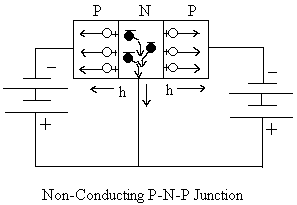
In this type of connection, holes in the each of p-region are attracted towards the negative battery terminal and the mobile electrons in the n-region are initially moved away from both junctions in the direction of the positive battery terminal. Due to the displacement of holes and electrons, there will be no current flow in the external circuit.
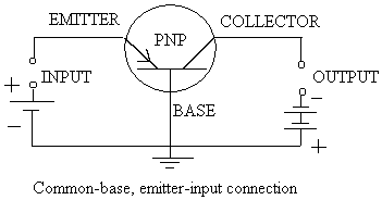
In the 2nd illustration, one of the p-n junctions is forward biased, while the other is reversed biased. In a transistor, the middle layer (here n-region) is called the base, the forward biased p-n junction is called the emitter junction and the reverse biased p-n junction is called collector junction. Due to the positive potential at the emitter junction, the holes in the p-region cross into the n-region (the base). But this region is very thin and there are very few electrons with which holes can combine. So, majority of the holes drift across the base into the collector junction. About 5 per cent of them are lost in the base region as they combine with electrons.
For each hole that is lost by combination with an electron in the base and collector areas, a covalent bond near the emitter electrode breaks down and a liberated electron leaves the emitter electrode and enters the positive battery terminal. The new hole that is formed then moves immediately toward the emitter junction, and the process is repeated.
Thus, a continuous supply of holes are injected into the emitter junction, which flow across the base region and collector junction, where they are gathered up by the negative collector voltage. The flow of current within the p-n-p transistor thus takes place by hole conduction from emitter to collector, while conduction in the external circuit is due to the conduction of electrons.
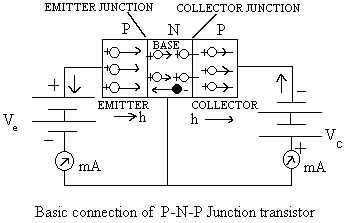
Because of the reverse bias no current can flow in the collector circuit, unless current is introduced into the emitter. Since a small emitter voltage of about 0.1 to 0.5 volt permits the flow of an appreciable emitter current, the input power to the emitter circuit is quite small. As we have seen, the collector current due to the diffusion of holes is almost as large as the emitter current. Moreover, the collector voltage can be as high as 45 volts, thus permitting relatively large output powers.
A large amount of power in the collector circuit may be controlled by a small amount of power in the emitter circuit. The power gain in a transistor (power out/power in) thus may be quite high, reaching values in the order of 1000.
The ratio of collector current to emitter current is known as alpha (a) and it is the measure of possible current amplification in a transistor. a cannot be higher than 1.
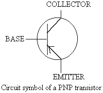
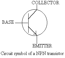
Transistor Symbols and Connection:
When transistors are operated as amplifier, three different basic circuit connections are possible: (a) Common-base, emitter input; (b) common-emitter, base input; and (c) common-collector, base-input.
Regardless of the circuit connection the emitter is always forward biased and collector is always reverse biased.
