The 555 timer IC was first introduced around 1971 by the Signetics Corporation as the SE555/NE555 and was called “The IC Time Machine” and was also the very first and only commercial timer ic available. It provided circuit designers and hobby tinkerers with a relatively cheap, stable, and user-friendly integrated circuit for both monostable and astable applications. Since this device was first made commercially available, a myrad of novel and unique circuits have been developed and presented in several trade, professional, and hobby publications. The past ten years some manufacturers stopped making these timers because of competition or other reasons. Yet other companies, like NTE picked up where some left off.
This primer is about this fantastic timer which is after 30 years still very popular and used in many schematics. Although these days the CMOS version of this IC, like the Motorola MC1455, is mostly used, the regular type is still available, however there have been many improvements and variations in the circuitry. But all types are pin-for-pin plug compatible. Myself, every time I see this 555 timer used in advanced and high-tech electronic circuits, I’m amazed. It is just incredible.
In this tutorial I will show you what exactly the 555 timer is and how to properly use it by itself or in combination with other solid state devices without the requirement of an engineering degree. This timer uses a maze of transistors, diodes and resistors and for this complex reason I will use a more simplified (but accurate) block diagram to explain the internal organizations of the 555. So, lets start slowly and build it up from there.
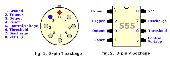
The 555, in fig. 1 and fig. 2 above, come in two packages, either the round metal-can called the ‘T’ package or the more familiar 8-pin DIP ‘V’ package. About 20-years ago the metal-can type was pretty much the standard (SE/NE types). The 556 timer is a dual 555 version and comes in a 14-pin DIP package, the 558 is a quad version with four 555’s also in a 14 pin DIP case.
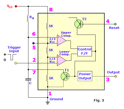 Inside the 555 timer, at fig. 3, are the equivalent of over 20 transistors, 15 resistors, and 2 diodes, depending of the manufacturer. The equivalent circuit, in block diagram, providing the functions of control, triggering, level sensing or comparison, discharge, and power output. Some of the more attractive features of the 555 timer are: Supply voltage between 4.5 and 18 volt, supply current 3 to 6 mA, and a Rise/Fall time of 100 nSec. It can also withstand quite a bit of abuse.
The Threshold current determine the maximum value of Ra + Rb. For 15 volt operation the maximum total resistance for R (Ra +Rb) is 20 Mega-ohm.
The supply current, when the output is ‘high’, is typically 1 milli-amp (mA) or less. The initial monostable timing accuracy is typically within 1% of its calculated value, and exhibits negligible (0.1%/V) drift with supply voltage. Thus long-term supply variations can be ignored, and the temperature variation is only 50ppm/°C (0.005%/°C).
 All IC timers rely upon an external capacitor to determine the off-on time intervals of the output pulses. As you recall from your study of basic electronics, it takes a finite period of time for a capacitor (C) to charge or discharge through a resistor (R). Those times are clearly defined and can be calculated given the values of resistance and capacitance.
The basic RC charging circuit is shown in fig. 4. Assume that the capacitor is initially discharged. When the switch is closed, the capacitor begins to charge through the resistor. The voltage across the capacitor rises from zero up to the value of the applied DC voltage. The charge curve for the circuit is shown in fig. 6. The time that it takes for the capacitor to charge to 63.7% of the applied voltage is known as the time constant (t). That time can be calculated with the simple expression:
t = R X C
Assume a resistor value of 1 Mega Ohm and a capacitor value of 1uF (micro-Farad). The time constant in that case is:
t = 1,000,000 X 0.000001 = 1 second
Assume further that the applied voltage is 6 volts. That means that it will take one time constant for the voltage across the capacitor to reach 63.2% of the applied voltage. Therefore, the capacitor charges to approximately 3.8 volts in one second.
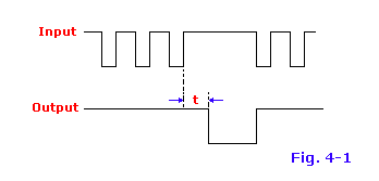 Fig. 4-1, Change in the input pulse frequency allows completion of the timing cycle. As a general rule, the monostable ‘ON’ time is set approximately 1/3 longer than the expected time between triggering pulses. Such a circuit is also known as a ‘Missing Pulse Detector’
Looking at the curve in fig. 6. you can see that it takes approximately 5 complete time constants for the capacitor to charge to amost the applied voltage. It would take about 5 seconds for the voltage on the capacitor to rise to approximately the full 6-volts.
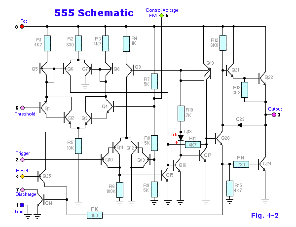
Refer to the internal 555 schematic of Fig. 4-2
Pin 1 (Ground): The ground (or common) pin is the most-negative supply potential of the device, which is normally connected to circuit common (ground) when operated from positive supply voltages.
Pin 2 (Trigger): This pin is the input to the lower comparator and is used to set the latch, which in turn causes the output to go high. This is the beginning of the timing sequence in monostable operation. Triggering is accomplished by taking the pin from above to below a voltage level of 1/3 V+ (or, in general, one-half the voltage appearing at pin 5). The action of the trigger input is level-sensitive, allowing slow rate-of-change waveforms, as well as pulses, to be used as trigger sources.
The trigger pulse must be of shorter duration than the time interval determined by the external R and C. If this pin is held low longer than that, the output will remain high until the trigger input is driven high again. One precaution that should be observed with the trigger input signal is that it must not remain lower than 1/3 V+ for a period of time longer than the timing cycle. If this is allowed to happen, the timer will retrigger itself upon termination of the first output pulse. Thus, when the timer is driven in the monostable mode with input pulses longer than the desired output pulse width, the input trigger should effectively be shortened by differentiation. The minimum-allowable pulse width for triggering is somewhat dependent upon pulse level, but in general if it is greater than the 1uS (micro-Second), triggering will be reliable. A second precaution with respect to the trigger input concerns storage time in the lower comparator.
This portion of the circuit can exhibit normal turn-off delays of several microseconds after triggering; that is, the latch can still have a trigger input for this period of time after the trigger pulse. In practice, this means the minimum monostable output pulse width should be in the order of 10uS to prevent possible double triggering due to this effect. The voltage range that can safely be applied to the trigger pin is between V+ and ground. A dc current, termed the trigger current, must also flow from this terminal into the external circuit. This current is typically 500nA (nano-amp) and will define the upper limit of resistance allowable from pin 2 to ground. For an astable configuration operating at V+ = 5 volts, this resistance is 3 Mega-ohm; it can be greater for higher V+ levels.
Pin 3 (Output): The output of the 555 comes from a high-current totem-pole stage made up of transistors Q20 – Q24. Transistors Q21 and Q22 provide drive for source-type loads, and their Darlington connection provides a high-state output voltage about 1.7 volts less than the V+ supply level used. Transistor Q24 provides current-sinking capability for low-state loads referred to V+ (such as typical TTL inputs).
Transistor Q24 has a low saturation voltage, which allows it to interface directly, with good noise margin, when driving current-sinking logic. Exact output saturation levels vary markedly with supply voltage, however, for both high and low states. At a V+ of 5 volts, for instance, the low state Vce(sat) is typically 0.25 volts at 5 mA. Operating at 15 volts, however, it can sink 200mA if an output-low voltage level of 2 volts is allowable (power dissipation should be considered in such a case, of course). High-state level is typically 3.3 volts at V+ = 5 volts; 13.3 volts at V+ = 15 volts.
Both the rise and fall times of the output waveform are quite fast, typical switching times being 100nS.The state of the output pin will always reflect the inverse of the logic state of the latch, and this fact may be seen by examining Fig. 3. Since the latch itself is not directly accessible, this relationship may be best explained in terms of latch-input trigger conditions. To trigger the output to a high condition, the trigger input is momentarily taken from a higher to a lower level. [see “Pin 2 – Trigger”].
This causes the latch to be set and the output to go high. Actuation of the lower comparator is the only manner in which the output can be placed in the high state. The output can be returned to a low state by causing the threshold to go from a lower to a higher level [see “Pin 6 – Threshold”], which resets the latch. The output can also be made to go low by taking the reset to a low state near ground [see “Pin 4 – Reset”]. The output voltage available at this pin is approximately equal to the Vcc applied to pin 8 minus 1.7V.
Pin 4 (Reset): This pin is also used to reset the latch and return the output to a low state. The reset voltage threshold level is 0.7 volt, and a sink current of 0.1mA from this pin is required to reset the device. These levels are relatively independent of operating V+ level; thus the reset input is TTL compatible for any supply voltage.
The reset input is an overriding function; that is, it will force the output to a low state regardless of the state of either of the other inputs. It may thus be used to terminate an output pulse prematurely, to gate oscillations from “on” to “off”, etc. Delay time from reset to output is typically on the order of 0.5 µS, and the minimum reset pulse width is 0.5 µS. Neither of these figures is guaranteed, however, and may vary from one manufacturer to another.
In short, the reset pin is used to reset the flip-flop that controls the state of output pin 3. The pin is activated when a voltage level anywhere between 0 and 0.4 volt is applied to the pin. The reset pin will force the output to go low no matter what state the other inputs to the flip-flop are in. When not used, it is recommended that the reset input be tied to V+ to avoid any possibility of false resetting.
Pin 5 (Control Voltage): This pin allows direct access to the 2/3 V+ voltage-divider point, the reference level for the upper comparator. It also allows indirect access to the lower comparator, as there is a 2:1 divider (R8 – R9) from this point to the lower-comparator reference input, Q13.
Use of this terminal is the option of the user, but it does allow extreme flexibility by permitting modification of the timing period, resetting of the comparator, etc.When the 555 timer is used in a voltage-controlled mode, its voltage-controlled operation ranges from about 1 volt less than V+ down to within 2 volts of ground (although this is not guaranteed). Voltages can be safely applied outside these limits, but they should be confined within the limits of V+ and ground for reliability. By applying a voltage to this pin, it is possible to vary the timing of the device independently of the RC network.
The control voltage may be varied from 45 to 90% of the Vcc in eh monostabel mode, making it possible to control the width of the output pulse independently of RC. When it is used in the astable mode, the control voltage can be varied from 1.7V to the full Vcc. Varying the voltage in the astable mode will produce a frequency modulated (FM) output. In the event the control-voltage pin is not used, it is recommended that it be bypassed, to ground, with a capacitor of about 0.01uF (10nF) for immunity to noise, since it is a comparator input.
This fact is not obvious in many 555 circuits since I have seen many circuits with ‘no-pin-5’ connected to anything, but this is the proper procedure. The small ceramic cap may eliminate false triggering.
Pin 6 (Threshold): Pin 6 is one input to the upper comparator (the other being pin 5) and is used to reset the latch, which causes the output to go low. Resetting via this terminal is accomplished by taking the terminal from below to above a voltage level of 2/3 V+ (the normal voltage on pin 5).
The action of the threshold pin is level sensitive, allowing slow rate-of-change waveforms. The voltage range that can safely be applied to the threshold pin is between V+ and ground. A dc current, termed the threshold current, must also flow into this terminal from the external circuit.
This current is typically 0.1µA, and will define the upper limit of total resistance allowable from pin 6 to V+. For either timing configuration operating at V+ = 5 volts, this resistance is 16 Mega-ohm. For 15 volt operation, the maximum value of resistance is 20 Mega Ohms.
Pin 7 (Discharge): This pin is connected to the open collector of a npn transistor (Q14), the emitter of which goes to ground, so that when the transistor is turned “on”, pin 7 is effectively shorted to ground. Usually the timing capacitor is connected between pin 7 and ground and is discharged when the transistor turns “on”. The conduction state of this transistor is identical in timing to that of the output stage.
It is “on” (low resistance to ground) when the output is low and “off” (high resistance to ground) when the output is high. In both the monostable and astable time modes, this transistor switch is used to clamp the appropriate nodes of the timing network to ground. Saturation voltage is typically below 100mV (milli-Volt) for currents of 5 mA or less, and off-state leakage is about 20nA (these parameters are not specified by all manufacturers, however). Maximum collector current is internally limited by design, thereby removing restrictions on capacitor size due to peak pulse-current discharge. In certain applications, this open collector output can be used as an auxiliary output terminal, with current-sinking capability similar to the output (pin 3).
Pin 8 (V +): The V+ pin (also referred to as Vcc) is the positive supply voltage terminal of the 555 timer IC. Supply-voltage operating range for the 555 is +4.5 volts (minimum) to +16 volts (maximum), and it is specified for operation between +5 volts and + 15 volts. The device will operate essentially the same over this range of voltages without change in timing period.
Actually, the most significant operational difference is the output drive capability, which increases for both current and voltage range as the supply voltage is increased. Sensitivity of time interval to supply voltage change is low, typically 0.1% per volt. There are special and military devices available that operate at voltages as high as 18 V.
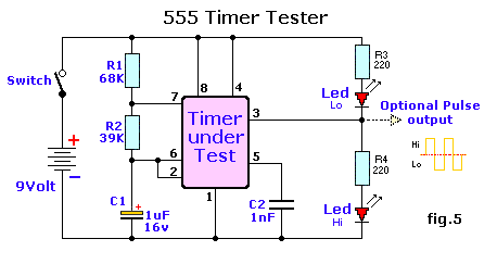 Try the simple 555 testing-circuit of Fig. 5. to get you going, and test all your 555 timer ic’s. I build several for friends and family. I bring my own tester to ham-fests and what not to instantly do a check and see if they are oscillating. Or use as a trouble shooter in 555 based circuits. This tester will quickly tell you if the timer is functional or not. Although not foolproof, it will tell if the 555 is shorted or oscillating. If both Led’s are flashing the timer is most likely in good working order. If one or both Led’s are either off or on solid the timer is defective. Simple huh?
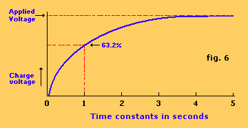 The capacitor slows down as it charges, and in actual fact never reaches the full supply voltage. That being the case, the maximum charge it receives in the timing circuit (66.6% of the supply voltage) is a little over the charge received after a time constant (63.2%).
 The capacitor slows down as it discharges, and never quite reaches the ground potential. That means the minimum voltage it operates at must be greater than zero. Timing circuit is 63.2% of the supply voltage.
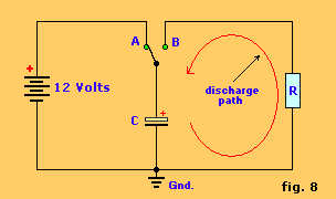 The discharge of a capacitor also takes time and we can shorten the amount of time by decreasing resistance (R) to the flow of current
The 555 timer has two basic operational modes: one shot and astable. In the one-shot mode, the 555 acts like a monostable multivibrator.
A monostable is said to have a single stable state–that is the off state. Whenever it is triggered by an input pulse, the monostable switches to its temporary state. It remains in that state for a period of time determined by an RC network. It then returns to its stable state. In other words, the monostable circuit generates a single pulse of a fixed time duration each time it receives and input trigger pulse. Thus the name one-shot.
One-shot multivibrators are used for turning some circuit or external component on or off for a specific length of time. It is also used to generate delays. When multiple one-shots are cascaded, a variety of sequential timing pulses can be generated. Those pulses will allow you to time and sequence a number of related operations. The other basic operational mode of the 555 is as and astable multivibrator.
An astable multivibrator is simply and oscillator. The astable multivibrator generates a continuous stream of rectangular off-on pulses that switch between two voltage levels. The frequency of the pulses and their duty cycle are dependent upon the RC network values.
One-Shot Operation: Fig. 4 shows the basic circuit of the 555 connected as a monostable multivibrator. An external RC network is connected between the supply voltage and ground. The junction of the resistor and capacitor is connected to the threshold input which is the input to the upper comparator. The internal discharge transistor is also connected to the junction of the resistor and the capacitor. An input trigger pulse is applied to the trigger input, which is the input to the lower comparator. With that circuit configuration, the control flip-flop is initially reset.
Therefore, the output voltage is near zero volts. The signal from the control flip-flop causes T1 to conduct and act as a short circuit across the external capacitor. For that reason, the capacitor cannot charge. During that time, the input to the upper comparator is near zero volts causing the comparator output to keep the control flip-flop reset.
Notice how the monostable continues to output its pulse regardless of the inputs swing back up. That is because the output is only triggered by the input pulse, the output actually depends on the capacitor charge.
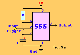 The 555 in fig. 9a is shown here in it’s utmost basic mode of operation; as a triggered monostable. One immediate observation is the extreme simplicity of this circuit. Only two components to make up a timer, a capacitor and a resistor. And for noise immunity maybe a capacitor on pin 5.
Due to the internal latching mechanism of the 555, the timer will always time-out once triggered, regardless of any subsequent noise (such as bounce) on the input trigger (pin 2). This is a great asset in interfacing the 555 with noisy sources. Just in case you don’t know what ‘bounce’ is: bounce is a type of fast, short term noise caused by a switch, relay, etc. and then picked up by the input pin.
The trigger input is initially high (about 1/3 of +V). When a negative-going trigger pulse is applied to the trigger input (see fig. 9a), the threshold on the lower comparator is exceeded. The lower comparator, therefore, sets the flip-flop. That causes T1 to cut off, acting as an open circuit. The setting of the flip-flop also causes a positive-going output level which is the beginning of the output timing pulse.
The capacitor now begins to charge through the external resistor. As soon as the charge on the capacitor equal 2/3 of the supply voltage, the upper comparator triggers and resets the control flip-flop. That terminates the output pulse which switches back to zero. At this time, T1 again conducts thereby discharging the capacitor. If a negative-going pulse is applied to the reset input while the output pulse is high, it will be terminated immediately as that pulse will reset the flip-flop.
Whenever a trigger pulse is applied to the input, the 555 will generate its single-duration output pulse. Depending upon the values of external resistance and capacitance used, the output timing pulse may be adjusted from approximately one millisecond to as high as on hundred seconds. For time intervals less than approximately 1-millisecond, it is recommended that standard logic one-shots designed for narrow pulses be used instead of a 555 timer. IC timers are normally used where long output pulses are required. In this application, the duration of the output pulse in seconds is approximately equal to: T = 1.1 x R x C (in seconds)
The output pulse width is defined by the above formula and with relatively few restrictions, timing components R(t) and C(t) can have a wide range of values. There is actually no theoretical upper limit on T (output pulse width), only practical ones. The lower limit is 10uS. You may consider the range of T to be 10uS to infinity, bounded only by R and C limits. Special R(t) and C(t) techniques allow for timing periods of days, weeks, and even months if so desired.
However, a reasonable lower limit for R(t) is in the order of about 10Kilo ohm, mainly from the standpoint of power economy. (Although R(t) can be lower that 10K without harm, there is no need for this from the standpoint of achieving a short pulse width.) A practical minimum for C(t) is about 95pF; below this the stray effects of capacitance become noticeable, limiting accuracy and predictability. Since it is obvious that the product of these two minimums yields a T that is less the 10uS, there is much flexibility in the selection of R(t) and C(t). Usually C(t) is selected first to minimize size (and expense); then R(t) is chosen.
The upper limit for R(t) is in the order of about 15 Mega ohm but should be less than this if all the accuracy of which the 555 is capable to be achieved. The absolute upper limit of R(t) is determined by the threshold current plus the discharge leakage when the operating voltage is +5 volt. For example, with a threshold plus leakage current of 120nA, this gives a maximum value of 14M for R(t) (very optimistic value). Also, if the C(t) leakage current is such that the sum of the threshold current and the leakage current is in excess of 120 nA the circuit will never time-out because the upper threshold voltage will not be reached. Therefore, it is good practice to select a value for R(t) so that, with a voltage drop of 1/3 V+ across it, the value should be 100 times more, if practical.
So, it should be obvious that the real limit to be placed on C(t) is its leakage, not it’s capacitance value, since larger-value capacitors have higher leakages as a fact of life. Low-leakage types, like tantalum or NPO, are available and preferred for long timing periods. Sometimes input trigger source conditions can exist that will necessitate some type of signal conditioning to ensure compatibility with the triggering requirements of the 555.
This can be achieved by adding another capacitor, one or two resistors and a small signal diode to the input to form a pulse differentiator to shorten the input trigger pulse to a width less than 10uS (in general, less than T). Their values and criterion are not critical; the main one is that the width of the resulting differentiated pulse (after C) should be less than the desired output pulse for the period of time it is below the 1/3 V+ trigger level.
There are several different types of 555 timers. The LM555 from National is the most common one these days, in my opinion. The Exar XR-L555 timer is a micropower version of the standard 555 offering a direct, pin-for-pin (also called plug-compatible) substitute device with an advantage of a lower power operation. It is capable of operation of a wider range of positive supply voltage from as low as 2.7volt minimum up to 18 volts maximum.
At a supply voltage of +5V, the L555 will typically dissipate of about 900 microwatts, making it ideally suitable for battery operated circuits. The internal schematic of the L555 is very much similar to the standard 555 but with additional features like ‘current spiking’ filtering, lower output drive capability, higher nodal impedances, and better noise reduction system.
Intersil’s ICM7555 model is a low-power, general purpose CMOS design version of the standard 555, also with a direct pin-for-pin compatibility with the regular 555. It’s advantages are very low timing/bias currents, low power-dissipation operation and an even wider voltage supply range of as low as 2.0 volts to 18 volts. At 5 volts the 7555 will dissipate about 400 microwatts, making it also very suitable for battery operation. The internal schematic of the 7555 (not shown) is however totally different from the normal 555 version because of the different design process with cmos technology.
It has much higher input impedances than the standard bipolar transistors used. The cmos version removes essentially any timing component restraints related to timer bias currents, allowing resistances as high as practical to be used. This very versatile version should be considered where a wide range of timing is desired, as well as low power operation and low current sync’ing appears to be important in the particular design.
A couple of years after Intersil, Texas Instruments came on the market with another cmos variation called the LINCMOS (LINear CMOS) or Turbo 555. In general, different manufacturers for the cmos 555’s reduced the current from 10mA to 100µA while the supply voltage minimum was reduced to about 2 volts, making it an ideal type for 3v applications.
The cmos version is the choice for battery powered circuits. However, the negative side for the cmos 555’s is the reduced output current, both for sync and source, but this problem can be solved by adding a amplifier transistor on the output if so required. For comparison, the regular 555 can easily deliver a 200mA output versus 5 to 50mA for the 7555. On the workbench the regular 555 reached a limited output frequency of 180Khz while the 7555 easily surpassed the 1.1Mhz mark and the TLC555 stopped at about 2.4Mhz. Components used were 1% Resistors and low-leakage capacitors, supply voltage used was 10volt.
Some of the less desirable properties of the regular 555 are high supply current, high trigger current, double output transitions, and inability to run with very low supply voltages. These problems have been remedied in a collection of CMOS successors.
A caution about the regular 555 timer chips; the 555, along with some other timer ic’s, generates a big (about 150mA) supply current glitch during each output transition. Be sure to use a hefty bypass capacitor over the power connections near the timer chip. And even so, the 555 may have a tendency to generate double output transitions.
Telephone System
 Astable operation: Figure 9b shows the 555 connected as an astable multivibrator. Both the trigger and threshold inputs (pins 2 and 6) to the two comparators are connected together and to the external capacitor. The capacitor charges toward the supply voltage through the two resistors, R1 and R2. The discharge pin (7) connected to the internal transistor is connected to the junction of those two resistors.
When power is first applied to the circuit, the capacitor will be uncharged, therefore, both the trigger and threshold inputs will be near zero volts (see Fig. 10). The lower comparator sets the control flip-flop causing the output to switch high. That also turns off transistor T1. That allows the capacitor to begin charging through R1 and R2. As soon as the charge on the capacitor reaches 2/3 of the supply voltage, the upper comparator will trigger causing the flip-flop to reset. That causes the output to switch low.
Transistor T1 also conducts. The effect of T1 conducting causes resistor R2 to be connected across the external capacitor. Resistor R2 is effectively connected to ground through internal transistor T1. The result of that is that the capacitor now begins to discharge through R2.
The only difference between the single 555, dual 556, and quad 558 (both 14-pin types), is the common power rail. For the rest everything remains the same as the single version, 8-pin 555.
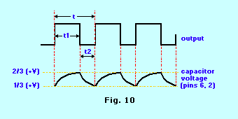 As soon as the voltage across the capacitor reaches 1/3 of the supply voltage, the lower comparator is triggered. That again causes the control flip-flop to set and the output to go high. Transistor T1 cuts off and again the capacitor begins to charge. That cycle continues to repeat with the capacitor alternately charging and discharging, as the comparators cause the flip-flop to be repeatedly set and reset. The resulting output is a continuous stream of rectangular pulses.
The frequency of operation of the astable circuit is dependent upon the values of R1, R2, and C. The frequency can be calculated with the formula: f = 1/(.693 x C x (R1 + 2 x R2))
The Frequency f is in Hz, R1 and R2 are in ohms, and C is in farads. The time duration between pulses is known as the ‘period’, and usually designated with a ‘t’. The pulse is on for t1 seconds, then off for t2 seconds. The total period (t) is t1 + t2 (see fig. 10).That time interval is related to the frequency by the familiar relationship
f = 1/t or t = 1/f
The time intervals for the on and off portions of the ouput depend upon the values of R1 and R2. The ratio of the time duration when the output pulse is high to the total period is known as the duty-cycle. The duty-cycle can be calculated with the formula: D = t1/t = (R1 + R2) / (R1 + 2R2)
You can calculate t1 and t2 times with the formulas:
t1 = .693(R1+R2)C
t2 = .693 x R2 x C
The 555, when connected as shown in Fig. 9b, can produce duty-cycles in the range of approximately 55 to 95%. A duty-cycle of 80% means that the output pulse is on or high for 80% of the total period. The duty-cycle can be adjusted by varying the values of R1 and R2.
Telephone System
There are literally thousands of different ways that the 555 can be used in electronic circuits. In almost every case, however, the basic circuit is either a one-shot or an astable. The application usually requires a specific pulse time duration, operation frequency, and duty-cycle. Additional components may have to be connected to the 555 to interface the device to external circuits or devices.
In the remainder of this experiment, you will build both the one-shot and astable circuits and learn about some of the different kinds of applications that can be implemented. Furthermore, the last page of this document contains 555 examples which you can build and experiment with.

