|
|
 |
|
| |
|
|
|
||||||||
|
|
|
|
What exactly is an OPerational AMPlifier? Let's define what that component is and look at the parameters of this amazing device. An operational amplifier IC is a solid-state integrated circuit that uses external feedback to control its functions. It is one of the most versatile devices in all of electronics. The term 'op-amp' was originally used to describe a chain of high performance dc amplifiers that was used as a basis for the analog type computers of long ago. The very high gain op-amp IC's our days uses external feedback networks to control responses. The op-amp without any external devices is called 'open-loop' mode, refering actually to the so-called 'ideal' operational amplifier with infinite open-loop gain, input resistance, bandwidth and a zero output resistance.However, in practice no op-amp can meet these ideal characteristics. And as you will see, a little later on, there is no such thing as an ideal op-amp.Since the LM741/NE741/µA741 Op-Amps are the most popular one, this tutorial is direct associated with this particular type. Nowadays the 741 is a frequency compensated device. The first op-amp offered to the public in 1963 was the µA702 manufactured by Fairchild Semiconductors but it had very weird supply voltages such as +12 and -6volts and had a tendency to burn out when it was temporarily shorted. Despite all these little shortcomings this device was the best in its day. In 1965 the next major change was introduced in op-amp design with the µA709 from Fairchild Semiconductor. It had higher gain, a larger bandwidth, lower input current, and a more user-friendly supply voltage requirement of approximately +15 Volt DC.National Semiconductor decided to jump on the bandwagen with the release of a more versatile op-amp version in the form of the LM101 in 1967. It had a an increased gain (up to 160K) and operation range. One of the nicest features of the LM101 was 'short-circuit' protection, and simplified frequency compensation. This was accomplished by placing an external capacitor across selected connection pins. The first op-amp to provide this internally was the hybrid LH101, which was basically a LM101 with a capacitor in a single package.But Fairchild was not done yet. It introduced in May 1968 an internally compensated op-amp called the µA741. However, the differences between their LM101 and the µA741 were very slight. Frequency compensation is accomplished using an 'on-chip' capacitor. Offset null is accomplished by adjustment of currents in input stage emitters. On the LM101, Offset is achieved by adjusting current in input stage collectors. In December 1968, an improved version of the LM101, the LM101A, was devised. This device provided better input control over the temperature and lower Offset currents.National Semiconductor introduced the LM107, which had the frequency compensation capacitor built into the silicon chip. The LM107 came out at the same time as the LM101A.In 1968, Fairchild Semiconductor issued the µA748. The device had essentially the same performance characteristics as the µA741. The difference was external frequency compensation. The first multiple op amp device was Raytheon Semiconductor's RC4558 in 1974. Characteristics of this new device are similar to the µA741 except that the latter uses NPN input transistors. Later in that same year, the LM324 quad op amp from National Semiconductor became public to the delight of manufacturing industry and hobbyist alike. It is similar in characteristics in comparison with the µA741 in speed and input current. The LM324 is especially useful for low-power consumption. The beauty of this chip, according to some engineers, is its single-power-supply requirement.Now the snowball was rolling. The first FET input op amp was the CA3130 made by RCA. With this addition to the op-amp family, extremely low input currents were achieved. Its power can be supplied by a +5 to +15vdc single supply system. A beautiful piece of work this CA3130.In July 1975, National Semiconductor came out with the J-FET type LF355. This was the first device created using ion implantation in an op amp.Texas Instruments introduced the TL084 op amp in October 1976. It is a quad JFET input op amp; it also is an ion-implant JFET. Low bias current and high speed are two of its beautiful attributes.In dated sequence, the op-amp developed like this: 1963-µA702, 1965-µA709, 1967-LM101/LH101, 1968-µA741, 1974-RC4558/LM324, 1975-CA3130/LF355, and in 1976 the TL084... Most of the mentioned op-amps have of course been replaced over time, keeping the same model number, with cleaner and low-noise types. Meaning, the silicon cutting laser in the early 60's was not of the same quality as the 70's or the 80's, etc. Other companies like RCA discontinued their semiconductor line all together.Today, and since that month in 1976, the types of op amps have increased almost daily. We now enjoy a variety of op amps that will provide the user essentially with anything s/he needs, such as high common-mode rejection, low-input current frequency compensation, cmos, and short-circuit protection. All a designer has to do is expressing his needs and is then supplied with the correct type. |
|
| ||||||||
|
|
|
|
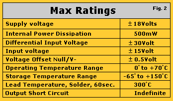
Absolute Maximum Parameters:Maximum means that the op-amp can safely tolerate the maximum ratings as given in the data section of such op-amp without the possibility of destroying it. The µA741 is a high performance operational amplifier with high open loop gain, internal compensation, high common mode range and exceptional temperature stability. The µA741 is short-circuit protected and allows for nulling of the offset voltage. The µA741 is Manufactured by Fairchild Semiconductor. |
|
|
|
|
|
|
Operating Temperature (Ta): This is the ambient temperature range for which the op-amp will operate within the manufacutre's specifications. Note that the military grade version (µA741)has a wider temperature range than the commercial, or hobbyist, grade version (µA741C). Output Short-Circuit Duration: This is the amount of time that an op-amp's ouput can be short-circuited to either supply voltage. Summed-up Features:Internal Frequency CompensationShort Circuit ProtectionOffset voltage null capabilityExcellent temperature stabilityHigh input voltage rangeNO latch-up Input Parameters: Input Offset Voltage (Voi)This is the voltage that must be applied to one of the input pins to give a zero output voltage. Remember, for an ideal op-amp, output offset voltage is zero! Input Bias Current (Ib)This is the average of the currents flowing into both inputs. Ideally, the two input bias currents are equal. Input Offset Current (Ios)This is the difference of the two input bias currents when the output voltage is zero. Input Voltage Range (Vcm)The range of the common-mode input voltage (i.e. the voltage common to both inputs and ground). Input Resistance (Zi)The resistance 'looking-in' at either input with the remaining input grounded. |
|
|
|
|
|
|
|
 |
|||||
|
Output Parameters: Output Resistance (Zoi)The resistance seen 'looking into' the op-amp's output. Output Short-Circuit Current (Iosc)This is the maximum output current that the op-amp can deliver to a load. Output Voltage Swing (Vo max)Depending on what the load resistance is, this is the maximum 'peak' output voltage that the op-amp can supply without saturation or clipping. Dynamic Parameters: Open-Loop Voltage Gain (Aol)The output to input voltage ratio of the op-amp without external feedback. Large-Signal Voltage GainThis is the ratio of the maximum voltage swing to the charge in the input voltage required to drive the ouput from zero to a specified voltage (e.g. 10 volts). Slew Rate (SR)The time rate of change of the ouput voltage with the op-amp circuit having a voltage gain of unity (1.0). Other Parameters: Supply CurrentThis is the current that the op-amp will draw from the power supply. Common-Mode Rejection Ratio (CMRR) A measure of the ability of the op-amp' to reject signals that are simultaneously present at both inputs. It is the ratio of the common-mode input voltage to the generated output voltage, usually expressed in decibels (dB). Channel SeperationWhenever there is more than one op-amp in a single package, like the 747 op-amp, a certain amount of "crosstalk" will be present. That is, a signal applied to the input of one section of a dual op-amp will produce a finite output signal in the remaining section, even though there is no input signal applied to the unused section. |
|||||
|
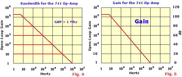
Open-Loop Gain & Frequency: |
|||||
 |
|||||
|
|
|
|
|
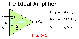
Unlike the ideal op-amp (Fig. 5-1), the op-amp that is used in more realistic circuits today, does not have infinite gain and bandwidth. Look at Open-loop gain in Fig. 4 above, it is graphed for a type 741 op-amp as a function of frequency. At very low frequencies, the open-loop gain of an op-amp is constant, but starts to taper off at about 6Hz or so at a rate of -6dB/octave or -20dB/decade (an octave is a doubling in frequency, and a decade is a ten-fold increase in frequency). This decrease continues until the gain is unity, or 0 dB. The frequency at which the gain is unity is called the unity gain frequency or fT.Maybe the first factor in the consideration of a specific op-amp is its "gain-bandwidth product" or GBP. For the response curve of Fig. 4, the product of the open-loop gain and frequency is a constant at any point on the curve, so that: GBP = AolBWGraphically, the bandwidth is the point at which the closed-loop gain curve intersects the open-loop curve, as shown in Fig. 5 for a family of closed-loop gains. For a more practical design situation, the actual design of an op-amp circuit should be approximately 1/10 to 1/20 of the open-loop gain at a given frequency. This ensures that the op-amp will function properly without distortion. As an example, using the response in Fig. 4, the closed-loop gain at 10Khz should be about 5 to 10, since the open-loop gain is 100 (40dB).One additional parameter is worth mentioning, the Transient Response, or rise time is the time that it takes for the output signal to go from 10% to 90% of its final value when a step-function pulse is used as an input signal, and is specified under close-loop condistions. From electronic circuit theory, the rise time is related to the bandwidth of the op-amp by the relation: BW = 0.35 / rise time Open-Loop Gain:Lets have a look how the 'ideal' amplifier would look like in Fig. 5-1. The search for an ideal amplifier is, of course, a futile exercise. The characteristics of the operational amplifier are good enough, however, to allow us to treat it as ideal. Below are some amplifier properties that make this so. (Please realize that these ratings are next to impossible to achieve). |
||
|
| |||||||||||||
|
|
|
|
|
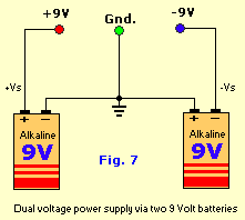
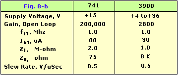
Power Supply:In general op-amps are designed to be powered from a dual or bipolar voltage supply which is typically in the range of +5V to +15Vdc with respect to ground, and another supply voltage of -5V to -15Vdc with respect to ground, as shown in Fig. 7. Although in certain cases an op-amp, like the LM3900 and called a 'Norton Op-Amp', may be powered from a single supply voltage. Electrical Ratings:Electrical characteristics for op-amps are usually specified for a certain (given) supply voltage and ambient temperature. Also, other factors may play an important role such as certain load and/or source resistance. In general, all parameters have a typical minimum/maximum value in most cases. |
||
|
| |||||||||||||
|
|
|
|
|
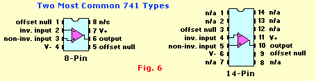
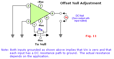
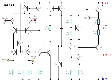
Definition of 741-pin functions: (Refer to the internal 741 schematic of Fig. 3) Pin 1 (Offset Null): Offset nulling, see Fig. 11. Since the op-amp is the differential type, input offset voltage must be controlled so as to minimize offset. Offset voltage is nulled by application of a voltage of opposite polarity to the ofset. An offset null-adjustment potentiometer may be used to compensate for offset voltage. The null-offset potentiometer also compensates for irregularities in the operational amplifier manufacturing process which may cause an offset. Consequently, the null potentiometer is recommended for critical applications. See 'Offset Null Adjustment' for method. Pin 2 (Inverted Input): All input signals at this pin will be inverted at output pin 6. Pins 2 and 3 are very important (obviously) to get the correct input signals or the op amp can not do its work. Pin 3 (Non-Inverted Input): All input signals at this pin will be processed normally without invertion. The rest is the same as pin 2. Pin 4 (-V): The V- pin (also referred to as Vss) is the negative supply voltage terminal. Supply-voltage operating range for the 741 is -4.5 volts (minimum) to -18 volts (max), and it is specified for operation between -5 and -15 Vdc. The device will operate essentially the same over this range of voltages without change in timing period. Sensitivity of time interval to supply voltage change is low, typically 0.1% per volt. (Note: Do not confuse the -V with ground). Pin 5 (Offset Null): See pin 1, and Fig. 11. Pin 6 (Output): Output signal's polarity will be the oposite of the input's when this signal is applied to the op-amp's inverting input. For example, a sine-wave at the inverting input will output a square-wave in the case of an inverting comparator circuit. Pin 7 (posV): The V+ pin (also referred to as Vcc) is the positive supply voltage terminal of the 741 Op-Amp IC. Supply-voltage operating range for the 741 is +4.5 volts (minimum) to +18 volts (maximum), and it is specified for operation between +5 and +15 Vdc. The device will operate essentially the same over this range of voltages without change in timing period. Actually, the most significant operational difference is the output drive capability, which increases for both current and voltage range as the supply voltage is increased. Sensitivity of time interval to supply voltage change is low, typically 0.1% per volt. Pin 8 (N/C): The 'N/C' stands for 'Not Connected'. There is no other explanation. There is nothing connected to this pin, it is just there to make it a standard 8-pin package. |
||
|
|
|
|
|
|
||
|
| ||||||||||||
|
|
|
|
|
Bread Board Modules:A bread board module, or just 'breadboard', is a board manufactured of plastic with a couple 100 tiny holes with tiny sockets in them connected electrically together and in the center of the breadboard a grove to hold a plastic panel for leds, pots and switches. They measure about 6 by 2 inches and come in white, gray and blue. The blue kind is called 'BimBoard' and made in the UK. I purchased mine back in 1980 from ElectroSonic in Toronto Canada and its still working fine. The gray and white models are manufactured in the U.S. and Canada. They all work.Radio Shack and the European Tandy are both selling their own version and they work fine too.The Bread Board Design System is also available, if you can afford it, and would be preferred if you intend to do a lot more experimenting in the future. This system contains everything you need already build-in, like the powersupply, jacks, switches, leds, function generator and lots more goodies. Kindah nice to have everything in one place.The Norton Op-Amp:It is not my intention to confuse you with a different type of op-amp so I will just mention a couple of points about this op-amp. The Norton op-amp, or current-differencing amplifier, is designed to operate from a single ended supply. Wow, that is truly fantastic. You can use a voltage anywhere from +4V to a whopping +36V! The Norton op-amp referred to here is the LM3900 and is the best known type made by National Semiconductor. This chip contains four op-amps in a single 14-pin package. The picture in Fig. 8-b below shows the symbol for the Norton op-amp. As you may notice it is somewhat different than the normal op-amp symbol. Fig. 8-c shows the major parameters of relevance between the 741 and the 3900 op-amps |
||
|
|
|
|
|
 |
|||
 |
|||
|
|
|
|
|
|
||
|
|
|
|
|
|
|
|
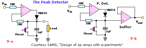
The Peak Detector The peak detector is a circuit that "remembers" the peak value of a signal. As shown in Fig. 9-a, when a positive voltage is fed to the noninverting input after the capacitor has been momentarily shorted (reset), the output voltage of the op-amp forward biases the diode and charges up the capacitor. This charging last until the inverting and noninverting inputs are at the same voltage, which is equal to the input voltage |
|||||
 |
|||||
|
. When the noninverting input voltage exceeds the voltage at the inverting input, which is also the voltage across the capacitor, the capacitor will charge up to the new peak value. Consequently, the capactor voltage will always be equal to the greatest positive voltage applied to the noninverting input.Once charged, the time that the peak detector "remembers" this peak value is typically several minutes and depends on the impedance of the load that is connected to the circuit. Consequently, the capacitor will slowly discharge towards zero. To minimize this rate of discharge, a voltage follower can be used to buffer the detector's output from any external load, as shown in Fig. 9-b. Momentarily shorting the capacitor to ground will immediately set the output to zero. |
|||||
|
|
|
|
|
|
||
|
|
|
|
|
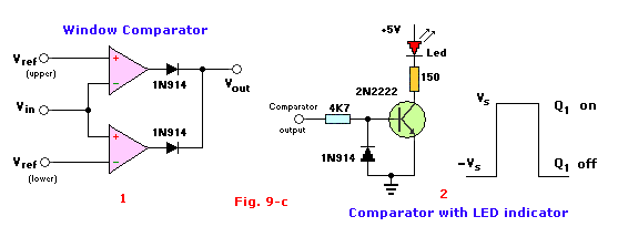
The ComparatorA 'comparator' is circuit that compares an input voltage with a reference voltage. The ouput of the comparator then indicates whether the input signal is either above or below the reference voltage. |
||
|
|
|
|
 |
||
|
|
|
|
|
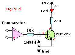
As shown for the basic circuit in Fig. 9-c(1), the output voltage approaches the positive supply voltage when the input signal is slightly greater than the reference voltage, Vref. When the input is slightly less than the reference, the op-amp's output approaches the negative supply voltage. Consequently, the exact threshold is dominated by the op-amp's input offset voltage, which should be nulled out. Fig. 9-c(2) shows a Led indicator wich input is connected to the output Vout of the comparator. |
||
|
| |||||||||||||||
|
|
|
|
|
|
||
|
|
|
|
|
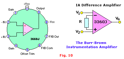
The Instrumentation AmplifierThere are many types of op-amps who are designed for a specific purpose like the Instrumentation Amplifier from Burr-Brown.(see Fig. 10) In this example we are talking about the 3660J type. It can be used in both balanced and unbalanced systems, like a Wheastone Bridge circuit. This does not mean in any way that the instrumentation amp cannot be used for other applications, on the contrary, it is in many a case prefered because of the unique parameters of this device. |
||
|
| |||||||||||||
|
|
|
|
|
Offset Null Adjustment Procedure for the µA741:Offset null adjustments differ with the application (e.i. Inverting or Non-Inverting Amplifier). Offset-null potentiometers are not placed on design schematics as they would detract from a design. For practice, perform the following Offset Null adjustment if you wish: |
||
|
| ||||||||||